Aim:
To practice
dataflow modelling and learn to write test benches using MODELSIM.
Data Flow Modeling:
Dataflow modeling makes use of the functions that define the
working of the circuit instead of its gate structure. Dataflow modeling has become a popular design
approach, as logic synthesis tools became sophisticated. This approach allows
the designer to focus on optimizing the circuit in terms of the flow of data. Dataflow modeling
uses several operators that act on operands to produce the desired results. Dataflow
modeling describes hardware in terms of the flow of data from input to output. The
dataflow modeling style is mainly used to describe combinational circuits. The
primary mechanism used is a continuous assignment.
Continuous Assignments
A value is assigned to a data type called net,
which is used to represent a physical connection between circuit elements in a
continuous assignment. The value assigned to the net is specified by an
expression that uses operands and operators.
A continuous assignment replaces gates in the circuit's
description and describes the circuit at a higher level of abstraction. A
continuous assignment statement starts with the keyword assign.
Syntax
The syntax of a continuous assignment is
assign [delay] LHS_net = RHS_expression;
LHS_net is a destination net of one or more bit, and
RHS_expression is an expression of various operators.
The statement is evaluated at any time any of the source
operand value changes, and the result is assigned to the destination net after
the delay unit.
·
The LHS of the assign statement must always be a
scalar or vector net or a concatenation. It cannot be a register.
·
Continuous statements are always active
statements, which means that if any value on the RHS changes, LHS changes
automatically.
·
Registers or nets or function calls can come in
the RHS of the assignment.
·
The RHS expression is evaluated whenever one of
its operand’s changes. Then the result is assigned to the LHS.
·
Delays can be specified in the assign statement.
assign out1 = in1 & in2; // perform and function on in1 and in2 and assign the result to out1
assign out2 = ~ in1;
Testbench:
A testbench is simply a
Verilog module. But it is different from the Verilog code we write for a DUT.
Since the DUT’s Verilog code is what we use for planning our hardware, it must
be synthesizable. Whereas, a testbench module need not be synthesizable. We
just need to simulate it to check the functionality of our DUT.
CODE:
|
Dataflow-level Code |
Testbench |
|
module and_gate (a, b, out); input a, b; output out; assign out = (a & b); endmodule |
module and_gate_testbench(); reg a,b; wire out; and_gate obj (a, b, out) initial begin a=0; b=0; #10 a=0; b=1; #10 a=1; b=0; #10 a=1; b=1; end endmodule |
Steps:
·
Like any Verilog code,
start with the module declaration.
·
In
testbench, we use reg for input and wire for output port.
o The reg datatype will hold the value until a new value is assigned
to it. This data type can be assigned a value only in the always or initial block.
This is used to apply a stimulus to the inputs of DUT.
o The wire datatype is similar to that of a physical connection. It
will hold the value that is driven by a port, assign statement, or reg. This
data type cannot be used in initial or always blocks.
This is used to check the output signals from the DUT.
o We can declare these data types for the testbench of the AND
module.
·
The purpose of a testbench is to verify whether
our DUT module is functioning as we wish. Hence, we have to instantiate our
design module to the test module. The format of the instantiation is: <dut_module>
<instance name>(.<dut_signal>(test_module_signal),…)
·
The initial block
The initial block is executed only once. It begins its execution at
the start of the simulation at time t = 0. The stimulus is written into
the initial block.
Here’s how we write stimulus
for and_gate in the initial block:
initialbeginA = 0; B = 0; // starts execution at t=0#10 A = 0; B = 1; // execution at t = 10-time units#10 A = 1; B = 0; // execution at t = 20-time units #10 A = 1; B = 1; //execution at t = 30-time units end
Starting
with the first line between the begin and end, each line executes from top to bottom until a delay is
reached. When the delay is reached, the execution of this block waits until the
delay time (10-time units) has passed and then picks up execution again.
We will try to do some task for practice:
01:
Write a Dataflow Verilog code for Half adder and Test bench for
simulation:
CODE:
module half_adder(x1,x2,out,c);
input x1,x2; output out,c; assign out = x1^x2;
assign
c = x1&x2;
endmodule module
half_adder_testbench();
reg x1,x2;
wire out,c;
half_adder obj(x1,x2,out,c);
initial
begin x1=0; x2=0;
#10 x1=0;x2=1;
#10
x1=1;x2=0; #10 x1=1;x2=1; end
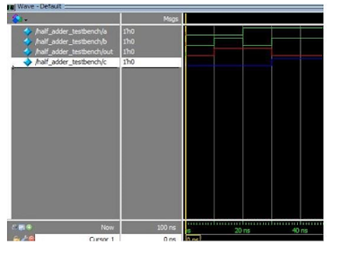
endmodule RESULT:
02:
Write a Dataflow Verilog code for Full adder calling module of half adder
and Test bench for simulation:
CODE:
module full_adder(x1,x2,cin,out,cout);
input x1,x2,cin;
output out,cout;
wire x21,x22,c;
half_adder obj1(x1,x2,x21,c);
half_adder obj2(x21,cin,out,x22);
assign
cout = c|x22;
endmodule
module
full_adder_testbench(); reg
x1,x2,cin;
wire out,cout;
full_adder
obj(x1,x2,cin,out,cout); initial
begin
x1=0;x2=0;cin=0;
#10 x1=0;x2=0;cin=1;
#10 x1=0;x2=1;cin=0;
#10 x1=0;x2=1;cin=1;
#10 x1=1;x2=0;cin=0;
#10 x1=1;x2=0;cin=1;
#10 x1=1;x2=1;cin=0; #10 x1=1;x2=1;cin=1; end
endmodule
RESULT:
DjshklHFKJhfjkLDHFjlhfjKLHFJKlhfiewuhfiAUFHCKJDfhkjdgfjdskgfksjdgfklGFJKSGFJSAGFJADSGFKJADSGFKJGSADKFGSAJDKFJKSADGFKJSDGFKJSDGFKJDSKFJDSGHFKJDSHFJKSADHFKJDSCBSDCBSDHFKJDSHFKJSHDFKJSHDFLASFLKJAGDFIUHFUISDGFJSDBCBDSJCGDSUIGFUIDSHKJSDHJKSDHKSJGFKJSDCSDJKBCDCBDJGJKDGFLAFJSLGFJDSGFJDSGHFUIX2UIFASHFKLHFDJADFJKLSDHFKLJSADHFLJK
SDHFLHDSFHDJSLFHJAKDSFKLDFHURIUWY893E8937WEHDSLCSCNCB8EY9843798723U99327490RUSJKDSDKLCJX1CNM


Thanks really appreciate 😍
ReplyDelete